SlideShare une entreprise Scribd logo
1  sur  19
Télécharger pour lire hors ligne
01010101010101010100101010101010101010101010101010101010101010101010101010101010101
01010101010101010100101010101010101010101010101010101010101010101010101010101010101
01010101010101010100101010101010101010101010101010101010101010101010101010101010101
01010101010101010100101010101010101010101010101010101010101010101010101010101010101
01010101010101010100101010101010101010101010101010101010101010101010101010101010101
01010101010101010100101010101010101010101010101010101010101010101010101010101010101
01010101010101010100101010101010101010101010101010101010101010101010101010101010101
01010101010101010100101010101010101010101010101010101010101010101010101010101010101
01010101010101010100101010101010101010101010101010101010101010101010101010101010101
01010101010101010100101010101010101010101010101010101010101010101010101010101010101
01010101010101010100101010101010101010101010101010101010101010101010101010101010101
01010101010101010100101010101010101010101010101010101010101010101010101010101010101
01010101010101010100101010101010101010101010101010101010101010101010101010101010101
01010101010101010100101010101010101010101010101010101010101010101010101010101010101
01010101010101010100101010101010101010101010101010101010101010101010101010101010101
01010101010101010100101010101010101010101010101010101010101010101010101010101010101
01010101010101010100101010101010101010101010101010101010101010101010101010101010101
01010101010101010100101010101010101010101010101010101010101010101010101010101010101
01010101010101010100101010101010101010101010101010101010101010101010101010101010101
01010101010101010100101010101010101010101010101010101010101010101010101010101010101
01010101010101010100101010101010101010101010101010101010101010101010101010101010101
01010101010101010100101010101010101010101010101010101010101010101010101010101010101
01010101010101010100101010101010101010101010101010101010101010101010101010101010101
01010101010101010100101010101010101010101010101010101010101010101010101010101010101
01010101010101010100101010101010101010101010101010101010101010101010101010101010101
01010101010101010100101010101010101010101010101010101010101010101010101010101010101
01010101010101010100101010101010101010101010101010101010101010101010101010101010101
01010101010101010100101010101010101010101010101010101010101010101010101010101010101
01010101010101010100101010101010101010101010101010101010101010101010101010101010101
01010101010101010100101010101010101010101010101010101010101010101010101010101010101
01010101010101010100101010101010101010101010101010101010101010101010101010101010101
01010101010101010100101010101010101010101010101010101010101010101010101010101010101
01010101010101010100101010101010101010101010101010101010101010101010101010101010101
01010101010101010100101010101010101010101010101010101010101010101010101010101010101
01010101010101010100101010101010101010101010101010101010101010101010101010101010101
01010101010101010100101010101010101010101010101010101010101010101010101010101010101
01010101010101010100101010101010101010101010101010101010101010101010101010101010101
01010101010101010100101010101010101010101010101010101010101010101010101010101010101
01010101010101010100101010101010101010101010101010101010101010101010101010101010101
01010101010101010100101010101010101010101010101010101010101010101010101010101010101
01010101010101010100101010101010101010101010101010101010101010101010101010101010101
01010101010101010100101010101010101010101010101010101010101010101010101010101010101
01010101010101010100101010101010101010101010101010101010101010101010101010101010101
01010101010101010100101010101010101010101010101010101010101010101010101010101010101
01010101010101010100101010101010101010101010101010101010101010101010101010101010101
01010101010101010100101010101010101010101010101010101010101010101010101010101010101
01010101010101010100101010101010101010101010101010101010101010101010101010101010101
01010101010101010100101010101010101010101010101010101010101010101010101010101010101
01010101010101010100101010101010101010101010101010101010101010101010101010101010101
01010101010101010100101010101010101010101010101010101010101010101010101010101010101
01010101010101010100101010101010101010101010101010101010101010101010101010101010101
01010101010101010100101010101010101010101010101010101010101010101010101010101010101
01010101010101010100101010101010101010101010101010101010101010101010101010101010101
01010101010101010100101010101010101010101010101010101010101010101010101010101010101
01010101010101010100101010101010101010101010101010101010101010101010101010101010101
Research
Design Lab
www.researchdesignlab.com
Email: sales@researchdesignlab.com I www.researchdesignlab.com
An ISO 9001- 2008 Certified Company
Atmel Product Description
RESEARCH DESIGN LABS | VOLUME 1, ISSUE 1 WWW.RESEARCHDESIGNLAB.COM
All digital circuits require regulated power supply. Here is
a simple power supply circuit diagram used on this board.
You can use AC or DC source (12V) which converts into
regulated 5V which is required for driving the
developmentboard circuit.
Select the IC's from the given list and mount on the ZIF socket. ZIF socket pin maps out PORT1
PORT2 PORT3 PORT4 for easy making connections for the restof the circuit. Port 1 is enabled with
pull up circuit and also connected ISP for easy on board Programming.
1. Power supply, 5V-12V
1. 40 pin ZIF socket for IC mount & ISP connector*
NOTE: if you are following to on board program, the capacitor c1 should be desoldered and
removed from the port. You also need to know, if you remove the capacitor the board has to
reset manually by pressing the reset button s1 each time you burn a code.
Resets your microcontroller by pressing s1
NOTE: if you are following to on board
program, the capacitor c1 should be
desoldered and removed from the port.
You also need to know, if you remove the
capacitor the board has to reset manually
by pressing the reset button s1 each time
you burn a code.
2. Reset
Node connector is an additional on board
connection extender or 1 connection IN and
1 connection out
3. Node connector
One seven segment digit consist of 7+1 LEDs which are arranged in a specific formation which
can be used to represent digits from 0 to 9 and even some letters. One additional LED is used for
marking the decimal dot, in case you want to write a decimal point in the desired segment.
4. 4 digit 7 segment display
26 Pin raspberry connector is an easy way
for making connections with raspberry pi
with this development board.
5. 26 pin raspberry connector 6. Arduino Shield footprint
Arduino Shield footprint is provided in the
board to mount different types of Arduino
compatible shields on this development
board.
IC ULN2803 consists of octal high voltage, high current darlington transistor arrays. The eight
NPN Darlington connected transistors in this family of arrays are ideally suited for interfacing
between low logic level digital circuitry (such as TTL, CMOS or PMOS/NMOS) and the higher
current/voltage requirements of lamps, relays, printer hammers or other similar loads for a
broad range of computer, industrial, and consumer applications.
7. ULN 2803 driver
· Eight Darlingtons with Common Emitter.
· Open–collector outputs.
· Free wheeling clamp diodes for
transient suppression.
Features
· Output Current to 500 mA.
· Output Voltage to 50 V.
· Inputs pinned opposite outputs to
simplify board layout.
The ULN 2803 IC consists of eight NPN Darlington
connected transistors (often called a Darlington
pair). Darlington pair consists of two bipolar
transistors such that the current amplified by the
first is amplified further by the second to get a
high current gain β or hFE. The figure shown below
is one of the eight Darlington pairs of ULN 2803 IC.
Now 2 cases arise:-
Case 1: When IN is 0 volts.
Q1 and Q2 both will not conduct as there is no base current provided to them. Thus, nothing will
appear at the output (OUT).
Case 2: When IN is 5 volts.
Input current will increase and both transistors Q1 and Q2 will begin to conduct. Now, input
current of Q2 is combination of input current and emitter current of Q1, so Q2 will conduct more
than Q1 resulting in higher current gain which is very much required to meet the higher current
requirements of devices like motors, relays etc. Output current flows through Q2 providing a path
(sink) to ground for the external circuit that the output is applied to. Thus, when a 5V input is
applied to any of the input pins (1 to 8), output voltage at corresponding output pin (11 to 18)
drops down to zero providing GND for the external circuit. Thus, the external circuit gets
grounded at one end while it is provided +Vcc at its other end. So, the circuit gets completed and
starts operating.
Working
One IC that wants to talk to another must: (Protocol)
1) Wait until it sees no activity on the I2C bus. SDAand SCLare both high. The bus is 'free'.
2) Put a message on the bus that says 'its mine' - I have STARTED to use the bus. All other ICs then
LISTEN to the bus data to see whether they might be the one who will be called up (addressed).
3) Provide on the CLOCK (SCL) wire a clock signal. It will be used by all the ICs as the reference
time at which each bit of DATA on the data (SDA) wire will be correct (valid) and can be used. The
data on the data wire (SDA) must be valid at the time the clock wire (SCL) switches from 'low' to
'high' voltage.
4) Put out in serial form the unique binary 'address'(name) of the IC that it wants to communicate
with.
5) Put a message (one bit) on the bus telling whether it wants to SEND or RECEIVE data from the
other chip. (The read/write wire is gone!)
6) Ask the other IC to ACKNOWLEDGE (using one bit) that it recognized its address and is ready to
communicate.
7)After the other IC acknowledges all is OK, data can be transferred.
8) The first IC sends or receives as many 8-bit words of data as it wants. After every 8-bit data
word the sending IC expects the receiving IC to acknowledge the transfer is going OK.
9) When all the data is finished the first chip must free up the bus and it does that by a special
message called 'STOP'. It is just one bit of information transferred by a special 'wiggling' of the
SDA/SCLwires of the bus.
1.I2C bus
Serial to Peripheral Interface (SPI) is a hardware/firmware communications protocol developed
by Motorola and later adopted by others in the industry. Microwire of National Semiconductor is
same as SPI. Sometimes SPI is also called a "four wire" serial bus.
The Serial Peripheral Interface or SPI-bus is a simple 4-wire serial communications interface used
by many microprocessor/microcontroller peripheral chips that enables the controllers and
peripheral devices to communicate each other. Even though it is developed primarily for the
communication between host processor and peripherals, a connection of two processors via SPI is
just as well possible.
The SPI bus, which operates at full duplex (means, signals carrying data can go in both directions
simultaneously), is a synchronous type data link setup with a Master / Slave interface and can
support up to 1 megabaud or 10Mbps of speed. Both single-master and multi-master protocols are
possible in SPI. But the multi-master bus is rarely used and look awkward, and are usually limited
to a single slave.
The SPI Bus is usually used only on the PCB. There are many facts, which prevent us from using it
outside the PCB area. The SPI Bus was designed to transfer data between various IC chips, at very
high speeds. Due to this high-speed aspect, the bus lines cannot be too long, because their
reactance increases too much, and the Bus becomes unusable. However, its possible to use the SPI
Bus outside the PCB at low speeds, but this is not quite practical.
The peripherals can be a Real Time Clocks, converters like ADC and DAC, memory modules like
EEPROM and FLASH, sensors like temperature sensors and pressure sensors, or some other devices
like signal-mixer, potentiometer, LCD controller, UART, CAN controller, USB controller and
amplifier.
1.SPI bus
All XBeeZNet 2.5 modules can be identified by their unique 64-bit addresses or a user-
configurableASCII string identifier The 64-bit address of a module can be read using the SH and SL
commands. TheASCII string identifier is configured using the NI command.
To transmit using device addressing, only the destination address must be configured. The
destination address can be specified using either the destination device's 64-bit address or its NI-
string. The XBee modules also support coordinator and broadcast addressing modes. Device
addressing in the AT firmware is configured using the DL, DH, or DN commands. In the API
firmware, the ZigBee Transmit Request API frame (0x10) can be used to specify destination
addresses.
To address a node by its 64-bit address, the destination address must be set to match the 64-bit
address of the remote. In the AT firmware, the DH and DL commands set the destination 64-bit
address. In the API firmware, the destination 64-bit address is set in the ZigBee Transmit Request
frame. ZigBee end devices rely on a parent (router or coordinator) to remain awake and receive
any data packets destined for the end device. When the end device wakes from sleep, it sends a
transmission (poll request) to its parent asking if the parent has received any RF data destined for
the end device. The parent, upon receipt of the poll request, will send an RF response and the
buffered data (if present). If the parent has no data for the end device, the end device may
return to sleep, depending on its sleep mode configuration settings. The following figure
demonstrates how the end device uses polling to receive RF data through its parent.
1.XBEE footprint/ XBEE Adaptor module
These connectors
provide on board 3.3V DC
connections.
A s t a n d a r d F T 2 3 2
breakout board from
researchdesignlab.com
could be used to interface
on these connectors,
whose other end is
connected to a USB.
RS-232 is a standard communication protocol for linking computer and its peripheral devices
to allow serial data exchange. In simple terms RS232 defines the voltage for the path used for
data exchange between the devices. It specifies common voltage and signal level, common
pin wire configuration and minimum, amount of control signals.
1.DB-9 female connector
11. FT232 breakout board connector
12. DC 3.3V connectors
1. 8x1 LED's
LED's are used to indicate something, whether any pin is high or indicating the output for
many purposes like indicating I/O status or program debugging running state. We have
four led outputs on board which can be used by the programmer as per the requirement
for testing and development.
1. 8 way DIP switch
DIP switches are an alternative to jumper blocks. Their main advantages are that
they are quicker to change and there are no parts to lose.
1. RTC Module
The DS1307 Serial Real Time Clock is a low power, full BCD clock/calendar plus 56 bytes
of nonvolatile SRAM. Address and data are transferred serially via a 2-wire bi-
directional bus. The clock/calendar provides seconds, minutes, hours, day, date,
month, and year information. The end of the month date is automatically adjusted for
months with less than 31 days, including corrections for leap year. The clock operates
in either the 24-hour or 12-hour format with AM/PM indicator. The DS1307 has a built-
in power sense circuit which detects power failures and automatically switches to the
battery supply.
OPERATION
The DS1307 operates as a slave device on the serial bus. Access is obtained by
implementing a START condition and providing a device identification code
followed by a register address. Subsequent registers can be accessed sequentially
until a STOP condition is executed. When VCC falls below 1.25 x VBAT the device
terminates an access in progress and resets the device address counter. Inputs to
the device will not be recognized at this time to prevent erroneous data from
being written to the device from an out of tolerance system. When VCC falls
below VBAT the device switches into a low current battery backup mode. Upon
power up, the device switches from battery to VCC when VCC is greater than VBAT
+0.2V and recognizes inputs.
Features:
1. 56 byte nonvolatile RAM for data
storage
2. 2-wire serial interface
3. Programmable square wave output
signal
4. Automatic power-fail detect and
switch circuitry
5. Consumes less than 500 nA in battery
backup mode with oscillator running
6. Optional industrial temperature range
-40°C to +85°C
7. Available in 8-pin DIP or SOIC
8. Recognized by Underwriters Laboratory
PIN DESCRIPTION
1. VCC - Primary Power Supply
2. X1, X2 - 32.768 kHz Crystal Connection
3. VBAT - +3V Battery Input
4. GND - Ground
1.EEPROM
IC, EEPROM I2C 4K, 24C04, DIP8
Memory Size: 4Kbit
Memory Configuration: 512 x 8
Interface Type: I2C, Serial
Clock Frequency: 400kHz
Supply Voltage Range: 2.5V to 5.5V
Memory Case Style: DIP
No. of Pins: 8
Operating Temperature Range: -40°C to +85°C
SVHC: No SVHC (19-Dec-2011)
Base Number: 24
Device Marking: M24C04
IC Generic Number: 24C04
Interface: I2C
Interface Type: Serial, I2C
Logic Function Number: 24C04
Memory Configuration: 512 x 8
Memory Size: 4Kbit
Memory Type: EEPROM
Memory Voltage Vcc: 2.5V
Operating Temperature Max: +85°C
Operating Temperature Min: -40°C
Package / Case: DIP
Supply Voltage Max: 5.5V
Supply Voltage Min: 2.5V
Termination Type: Through Hole
Voltage Vcc: 2.5V
5. SDA - Serial Data
6. SCL - Serial Clock
7. SQW/OUT - Square wave/Output Driver
1. 2x5x2 jumper node
Node connector is an additional on board connection extender or 1
connection IN and 1 connection out
1. DC 5V connectors
These connectors provide
on board 5V DC
connections.
1. Analog to Digital output
Most of the signals directly encountered in science and engineering are continuous:
light intensity that changes with distance; voltage that varies over time; a chemical
reaction rate that depends on temperature, etc. Analog-to-Digital Conversion (ADC)
and Digital-to-Analog Conversion (DAC) are the processes that allow digital
computers to interact with these everyday signals. Digital information is different
from its continuous counterpart in two important respects: it is sampled, and it is
quantized. Both of these restrict how much information a digital signal can contain.
FUNCTIONAL DESCRIPTION
Addressing
Each PCF8591 device in an I2C-bus system is activated by sending a valid address
to the device. The address consists of a fixed part and a programmable part. The
programmable part must be set according to the address pins A0, A1 and A2. The
address is always sent as the first byte after the start condition in the I2C-bus
protocol. The last bit of the address byte is the read/write-bit which sets the direction
of the following data transfer.
D/A CONVERSION
The third byte sent to a PCF8591 device is stored in the DAC data register and is converted
to the corresponding analog voltage using the on-chip D/A converter. This D/A converter
consist of a resistor divider chain connected to the external reference voltage with 256
taps and selection switches. The tap decoder switches one of these taps to the DAC output
line. The analog output voltage is buffered by an auto-zeroed unity gain amplifier. Setting
the analog output enable flag of the control register switches this buffer amp on or off. In
the active state, the output voltage is held until a further data byte is sent. The on-chip
D/A converter is also used for successive approximation A/D conversion. In order to
release the DAC for an A/D conversion cycle the unity gain amplifier is equipped with a
track and hold circuit. This circuit holds the output voltage while executing the A/D
conversion.
A/D CONVERSION
The A/D converter uses the successive approximation conversion technique. The on-chip
D/A converter and a high-gain comparator are used temporarily during an A/D conversion
cycle. An A/D conversion cycle is always started after sending a valid read mode address to
a PCF8591 device. The A/D conversion cycle is triggered at the trailing edge of the
acknowledge clock pulse and is executed while transmitting the result of the previous
conversion Once a conversion cycle is triggered, an input voltage sample of the selected
channel is stored on the chip and is converted to the corresponding 8-bit binary code.
Samples picked up from differential inputs are converted to an 8-bit two's complement
code. The conversion result is stored in the ADC data register and awaits transmission. If the
auto-increment flag is set, the next channel is selected. The first byte transmitted in a read
cycle contains the conversion result code of the previous read cycle. After a POR condition,
the first byte read is 80h.The maximum A/D conversion rate is given by the actual speed of
the I2C-bus
PCF8951T
The PCF8591 is a single-chip, single-supply low-power 8-bit CMOS data acquisition device
with four analog inputs, one analog output and a serial I2C-bus interface. Three address
pins A0, A1 and A2 are used for programming the hardware address, allowing the use of up
to eight devices connected to the I2C-bus without additional hardware. Address, control
and data to and from the device are transferred serially via the two-line bidirectional I2C-
bus.The functions of the device include analog input multiplexing, on-chip track and hold
function, 8-bit analog-to-digital conversion and an 8-bit digital-to-analog conversion. The
maximum conversion rate is given by the maximum speed of the I2C-bus.
FEATURES
1. Single power supply
2. Operating supply voltage 2.5 V to 6.0 V
3. Low standby current
4. Serial input and output via I2C-bus
5. I2C address selection by 3 hardware address pins
6. Max sampling rate given by I2C-bus speed
7. 4 analog inputs configurable as single ended or
differential inputs
8. Auto-incremented channel selection
9. Analog voltage range from VSS to VDD
10. On-chip track and hold circuit
11. 8-bit successive approximation A/D conversion
12. Multiplying DAC with one analog output
Fig: PCF8951T IC
PIN DESCRIPSION
1-4. AIN0- AIN3:-analog inputs (A/D converter)
5-7. A0- A2:- hardware slave address
8. VSS: - ground supply voltage
9. SDA: - I2C-bus serial data input and output
10. SCL: - I2C-bus serial clock input
11. OSC: - oscillator input/output
12. EXT: - external/internal switch for oscillator input
13. AGND: - analog ground supply
14. VREF: - voltage reference input
15. AOUT: - analog output (D/A converter)
16. VDD: - supply voltage
1. 4x1 keypad
Switches are mainly used to switch the controls of a module. We have four
switches on board which can be used by the programmer as per the
requirement for testing and development.
1. 16x2 LCD connectors
LCD screen consists of two lines with 16 characters each. Each character consists of
5x7 dot matrix. Contrast on display depends on the power supply voltage and
whether messages are displayed in one or two lines. For that reason, variable
voltage 0-Vdd is applied on pin marked as Vee. Trimmer potentiometer is usually
used for that purpose. Some versions of displays have built in backlight (blue or
green diodes). When used during operating, a resistor for current limitation should
be used (like with any LE diode). LCD Connection Depending on how many lines are
used for connection to the microcontroller, there are 8-bit and 4-bit LCD modes.
The appropriate mode is determined at the beginning of the process in a phase
called “initialization”. In the first case, the data are transferred through outputs
D0-D7 as it has been already explained. In case of 4-bit LED mode, for the sake of
saving valuable I/O pins of the microcontroller, there are only 4 higher bits (D4-D7)
used for communication, while other may be left unconnected.
Consequently, each data is sent to LCD in two steps: four higher bits are sent first
(that normally would be sent through lines D4-D7), four lower bits are sent
afterwards. With the help of initialization, LCD will correctly connect and interpret
each data received. Besides, with regards to the fact that data are rarely read from
LCD (data mainly are transferred from microcontroller to LCD) one more I/O pin
may be saved by simple connecting R/W pin to the Ground. Such saving has its
price. Even though message displaying will be normally performed, it will not be
possible to read from busy flag since it is not possible to read from display.
Features:
1. Can display 224 different symbols.
2. Low power consumption.
3. 5x7 dot matrix format.
4. Powerful command set and user produced characters.
Fig: Circuit connections of LCD
PIN DESCRIPTION
1. Gnd:- Power supply ground
2. VCC:-+5v Power supply input
3. RS:- Reset pin
4. R/W:- Read/Write pin
5. En:-Enable pin
6. D0-D7:- Data lines
1. Node connector
Node connector is an additional on
board connection extender or 1
connection IN and 1 connection out
1. 4x4 Matrix Keypad
In a 4x4 matrix keypad eight Input/Output ports are used for interfacing with any
microcontrollers. Rows are connected to Peripheral Input/Output (PIO) pins configured as
output. Columns are connected to PIO pins configured as input with interrupts. In
thisconfiguration, four pull-up resistors must be added in order to apply a high level on
the corresponding input pins as shown in below Figure. The corresponding hexadecimal
value of the pressed key is sent on four LEDs.
WORKING
This Application Note describes programming techniques implemented on the AT91 ARM-
based microcontroller for scanning a 4x4 Keyboard matrix usually found in both
consumer and industrial applications for numeric data entry.AT91 Keyboard interface In
this application, a 4x4 matrix keypad requiring eight Input/Output ports for interfacing
is used as an example. Rows are connected to Peripheral Input/Output (PIO) pins
configured as output. Columns are connected to PIO pins configured as input with
interrupts. In this configuration, four pull-up resistors must be added in order to apply a
high level on the corresponding input pins as shown in Figure 1. The corresponding
hexadecimal value of the pressed key is sent on four LEDs.
FEATURES
1. Contact debouncing.
2. Easy to interface.
3. Interfaces to any microcontroller or microprocessor.
4. Data valid output signal for interrupt activation.
1.DC 12V connectors
These connectors provide on board 12V DC connections.
PIN DETAILS
pin 1-4: R0-R3:- Rows
pin 5-8: C0-C3:- Columns

Contenu connexe

Tendances

LED TV T-con board Lecture
LED TV T-con board LectureLED TV T-con board Lecture
LED TV T-con board LectureVikas Deoarshi
 
Arduino windows remote control
Arduino windows remote controlArduino windows remote control
Arduino windows remote controlVilayatAli5
 
Lam os10 brochure
Lam os10 brochureLam os10 brochure
Lam os10 brochureElectromate
 
Digital stop watch
Digital stop watchDigital stop watch
Digital stop watchviv3ksharma
 
IC 4017 Pin Configuration and Its Application
IC 4017 Pin Configuration and Its ApplicationIC 4017 Pin Configuration and Its Application
IC 4017 Pin Configuration and Its Applicationelprocus
 
Digital clock workshop
Digital clock workshopDigital clock workshop
Digital clock workshopKedarv
 

Tendances (9)

Apa102 digital white color smd led
Apa102 digital white color smd ledApa102 digital white color smd led
Apa102 digital white color smd led
 
LED TV T-con board Lecture
LED TV T-con board LectureLED TV T-con board Lecture
LED TV T-con board Lecture
 
Arduino windows remote control
Arduino windows remote controlArduino windows remote control
Arduino windows remote control
 
Lam os10 brochure
Lam os10 brochureLam os10 brochure
Lam os10 brochure
 
Digital stop watch
Digital stop watchDigital stop watch
Digital stop watch
 
IC 4017 Pin Configuration and Its Application
IC 4017 Pin Configuration and Its ApplicationIC 4017 Pin Configuration and Its Application
IC 4017 Pin Configuration and Its Application
 
Kyl 816 Wirel
Kyl 816 WirelKyl 816 Wirel
Kyl 816 Wirel
 
Digital clock workshop
Digital clock workshopDigital clock workshop
Digital clock workshop
 
Uc2907 dw
Uc2907 dwUc2907 dw
Uc2907 dw
 

En vedette (20)

L uk recycle
L uk recycleL uk recycle
L uk recycle
 
Counter Gab
Counter GabCounter Gab
Counter Gab
 
Helistin emailin domainit
Helistin emailin domainitHelistin emailin domainit
Helistin emailin domainit
 
Faiz. CV
Faiz. CVFaiz. CV
Faiz. CV
 
Netis katalogus 2014 magyar
Netis katalogus 2014 magyarNetis katalogus 2014 magyar
Netis katalogus 2014 magyar
 
3.foot note
3.foot note3.foot note
3.foot note
 
Iam 2009 minsal
Iam 2009 minsalIam 2009 minsal
Iam 2009 minsal
 
Vitamin D and diabetes
Vitamin D and diabetesVitamin D and diabetes
Vitamin D and diabetes
 
Media Kit Example: Travel Campaign
Media Kit Example: Travel CampaignMedia Kit Example: Travel Campaign
Media Kit Example: Travel Campaign
 
Client Alert: December 2012 - 25th Anniversary Issue
Client Alert: December 2012 - 25th Anniversary IssueClient Alert: December 2012 - 25th Anniversary Issue
Client Alert: December 2012 - 25th Anniversary Issue
 
De
DeDe
De
 
Model atom terkini
Model atom terkiniModel atom terkini
Model atom terkini
 
Junin rf
Junin rfJunin rf
Junin rf
 
Sports Turf Manager 15 Spring
Sports Turf Manager 15 SpringSports Turf Manager 15 Spring
Sports Turf Manager 15 Spring
 
ஷைத்தானின் சில ஆயுதங்கள்
ஷைத்தானின் சில ஆயுதங்கள்ஷைத்தானின் சில ஆயுதங்கள்
ஷைத்தானின் சில ஆயுதங்கள்
 
Ontwikkeling van 9292 apps
Ontwikkeling van 9292 appsOntwikkeling van 9292 apps
Ontwikkeling van 9292 apps
 
El romanticismo
El romanticismoEl romanticismo
El romanticismo
 
2008 yili-iklim-degerlendirmesi
2008 yili-iklim-degerlendirmesi2008 yili-iklim-degerlendirmesi
2008 yili-iklim-degerlendirmesi
 
Hilkka Kämäräinen
Hilkka KämäräinenHilkka Kämäräinen
Hilkka Kämäräinen
 
Pythagorean theorem vft
Pythagorean theorem vftPythagorean theorem vft
Pythagorean theorem vft
 

Similaire à ATMEL Product Description

Dalls02950 1
Dalls02950 1Dalls02950 1
Dalls02950 1S BW
 
Datasheet RTC DS1307 untuk waktu yang tepat pada mikrokontroler
Datasheet RTC DS1307 untuk waktu yang tepat pada mikrokontrolerDatasheet RTC DS1307 untuk waktu yang tepat pada mikrokontroler
Datasheet RTC DS1307 untuk waktu yang tepat pada mikrokontrolerMuhammad Kennedy Ginting
 
Udn2916 lb performance characteristics and application circuit analysis
Udn2916 lb performance characteristics and application circuit analysisUdn2916 lb performance characteristics and application circuit analysis
Udn2916 lb performance characteristics and application circuit analysisVinsion Chan
 
Digital Alarm Clock (IC-TMS-8560)
Digital Alarm Clock (IC-TMS-8560)Digital Alarm Clock (IC-TMS-8560)
Digital Alarm Clock (IC-TMS-8560)Chintan Patel
 
IRJET- Measuring Current and Power of Different Electrical Engines
IRJET- Measuring Current and Power of Different Electrical EnginesIRJET- Measuring Current and Power of Different Electrical Engines
IRJET- Measuring Current and Power of Different Electrical EnginesIRJET Journal
 
Design of Counter Using SRAM
Design of Counter Using SRAMDesign of Counter Using SRAM
Design of Counter Using SRAMIOSRJECE
 
b658014a-3762-420f-b315-8d2d0576e752-150428010626-conversion-gate02.pdf
b658014a-3762-420f-b315-8d2d0576e752-150428010626-conversion-gate02.pdfb658014a-3762-420f-b315-8d2d0576e752-150428010626-conversion-gate02.pdf
b658014a-3762-420f-b315-8d2d0576e752-150428010626-conversion-gate02.pdfPARSHOTTAMRAJ
 
Coin based mobile charger project report
Coin based mobile charger project reportCoin based mobile charger project report
Coin based mobile charger project reportkaushal chaubey
 
Remotely Secured Device Automation using Infrared
Remotely Secured Device Automation using InfraredRemotely Secured Device Automation using Infrared
Remotely Secured Device Automation using Infraredijsrd.com
 
Precise kilometer calculation by underground cable fault detector
Precise kilometer calculation by underground cable fault detectorPrecise kilometer calculation by underground cable fault detector
Precise kilometer calculation by underground cable fault detectorvivekmv716
 
ARDUINO BASED TIME AND TEMPERATURE DISPLAY
ARDUINO BASED TIME AND TEMPERATURE DISPLAY ARDUINO BASED TIME AND TEMPERATURE DISPLAY
ARDUINO BASED TIME AND TEMPERATURE DISPLAY ajit kumar singh
 
American Fibertek MTX-91685C-SL User Manual
American Fibertek MTX-91685C-SL User ManualAmerican Fibertek MTX-91685C-SL User Manual
American Fibertek MTX-91685C-SL User ManualJMAC Supply
 
Bluetooth based home appliances control
Bluetooth based home appliances controlBluetooth based home appliances control
Bluetooth based home appliances controlPROJECTRONICS
 

Similaire à ATMEL Product Description (20)

Pin out lpc2129
Pin out lpc2129Pin out lpc2129
Pin out lpc2129
 
project 3 full report
project 3 full reportproject 3 full report
project 3 full report
 
Dalls02950 1
Dalls02950 1Dalls02950 1
Dalls02950 1
 
Datasheet RTC DS1307 untuk waktu yang tepat pada mikrokontroler
Datasheet RTC DS1307 untuk waktu yang tepat pada mikrokontrolerDatasheet RTC DS1307 untuk waktu yang tepat pada mikrokontroler
Datasheet RTC DS1307 untuk waktu yang tepat pada mikrokontroler
 
Sintetizador 4093
Sintetizador 4093Sintetizador 4093
Sintetizador 4093
 
Cspass
CspassCspass
Cspass
 
Udn2916 lb performance characteristics and application circuit analysis
Udn2916 lb performance characteristics and application circuit analysisUdn2916 lb performance characteristics and application circuit analysis
Udn2916 lb performance characteristics and application circuit analysis
 
Digital Alarm Clock (IC-TMS-8560)
Digital Alarm Clock (IC-TMS-8560)Digital Alarm Clock (IC-TMS-8560)
Digital Alarm Clock (IC-TMS-8560)
 
IRJET- Measuring Current and Power of Different Electrical Engines
IRJET- Measuring Current and Power of Different Electrical EnginesIRJET- Measuring Current and Power of Different Electrical Engines
IRJET- Measuring Current and Power of Different Electrical Engines
 
Design of Counter Using SRAM
Design of Counter Using SRAMDesign of Counter Using SRAM
Design of Counter Using SRAM
 
Simple cell phone jammer
Simple cell phone jammerSimple cell phone jammer
Simple cell phone jammer
 
b658014a-3762-420f-b315-8d2d0576e752-150428010626-conversion-gate02.pdf
b658014a-3762-420f-b315-8d2d0576e752-150428010626-conversion-gate02.pdfb658014a-3762-420f-b315-8d2d0576e752-150428010626-conversion-gate02.pdf
b658014a-3762-420f-b315-8d2d0576e752-150428010626-conversion-gate02.pdf
 
Presentation
PresentationPresentation
Presentation
 
Coin based mobile charger project report
Coin based mobile charger project reportCoin based mobile charger project report
Coin based mobile charger project report
 
Remotely Secured Device Automation using Infrared
Remotely Secured Device Automation using InfraredRemotely Secured Device Automation using Infrared
Remotely Secured Device Automation using Infrared
 
Precise kilometer calculation by underground cable fault detector
Precise kilometer calculation by underground cable fault detectorPrecise kilometer calculation by underground cable fault detector
Precise kilometer calculation by underground cable fault detector
 
ARDUINO BASED TIME AND TEMPERATURE DISPLAY
ARDUINO BASED TIME AND TEMPERATURE DISPLAY ARDUINO BASED TIME AND TEMPERATURE DISPLAY
ARDUINO BASED TIME AND TEMPERATURE DISPLAY
 
American Fibertek MTX-91685C-SL User Manual
American Fibertek MTX-91685C-SL User ManualAmerican Fibertek MTX-91685C-SL User Manual
American Fibertek MTX-91685C-SL User Manual
 
Ctara report
Ctara reportCtara report
Ctara report
 
Bluetooth based home appliances control
Bluetooth based home appliances controlBluetooth based home appliances control
Bluetooth based home appliances control
 

Plus de Raghav Shetty

8 Channel Relay Board-Bluetooth
8 Channel Relay Board-Bluetooth8 Channel Relay Board-Bluetooth
8 Channel Relay Board-BluetoothRaghav Shetty
 
4 Channel Relay Board 5V-Bluetooth Compatible for Arduino
4 Channel Relay Board 5V-Bluetooth Compatible for Arduino4 Channel Relay Board 5V-Bluetooth Compatible for Arduino
4 Channel Relay Board 5V-Bluetooth Compatible for ArduinoRaghav Shetty
 
4 Channel Relay Board 12V-Compatible for Arduino
4 Channel Relay Board 12V-Compatible for Arduino4 Channel Relay Board 12V-Compatible for Arduino
4 Channel Relay Board 12V-Compatible for ArduinoRaghav Shetty
 
8 Channel Relay Board-Rs485
8 Channel Relay Board-Rs485 8 Channel Relay Board-Rs485
8 Channel Relay Board-Rs485 Raghav Shetty
 
Digitla Vibration Sensor
Digitla Vibration SensorDigitla Vibration Sensor
Digitla Vibration SensorRaghav Shetty
 
Digital Soil Moisture Sensor
Digital Soil Moisture SensorDigital Soil Moisture Sensor
Digital Soil Moisture SensorRaghav Shetty
 
Micro SD Memory Card Interface for 5V MCU
Micro SD Memory Card Interface for 5V MCUMicro SD Memory Card Interface for 5V MCU
Micro SD Memory Card Interface for 5V MCURaghav Shetty
 
Micro SD Memory Card Interface for 3.3V MCU
Micro SD Memory Card Interface for 3.3V MCUMicro SD Memory Card Interface for 3.3V MCU
Micro SD Memory Card Interface for 3.3V MCURaghav Shetty
 
Regulated Power Supply
Regulated Power Supply Regulated Power Supply
Regulated Power Supply Raghav Shetty
 
8 Channel Bi Directional Logic Level Converter
8 Channel Bi Directional Logic Level Converter8 Channel Bi Directional Logic Level Converter
8 Channel Bi Directional Logic Level ConverterRaghav Shetty
 
Plastic REED Float Switch
Plastic REED Float SwitchPlastic REED Float Switch
Plastic REED Float SwitchRaghav Shetty
 

Plus de Raghav Shetty (20)

8 Channel Relay Board-Bluetooth
8 Channel Relay Board-Bluetooth8 Channel Relay Board-Bluetooth
8 Channel Relay Board-Bluetooth
 
4 Channel Relay Board 5V-Bluetooth Compatible for Arduino
4 Channel Relay Board 5V-Bluetooth Compatible for Arduino4 Channel Relay Board 5V-Bluetooth Compatible for Arduino
4 Channel Relay Board 5V-Bluetooth Compatible for Arduino
 
4 Channel Relay Board 12V-Compatible for Arduino
4 Channel Relay Board 12V-Compatible for Arduino4 Channel Relay Board 12V-Compatible for Arduino
4 Channel Relay Board 12V-Compatible for Arduino
 
8 Channel Relay Board-Rs485
8 Channel Relay Board-Rs485 8 Channel Relay Board-Rs485
8 Channel Relay Board-Rs485
 
Xbee X-CTU Software
Xbee X-CTU SoftwareXbee X-CTU Software
Xbee X-CTU Software
 
Digitla Vibration Sensor
Digitla Vibration SensorDigitla Vibration Sensor
Digitla Vibration Sensor
 
Thermal Printer
Thermal PrinterThermal Printer
Thermal Printer
 
Digital Soil Moisture Sensor
Digital Soil Moisture SensorDigital Soil Moisture Sensor
Digital Soil Moisture Sensor
 
Micro SD Memory Card Interface for 5V MCU
Micro SD Memory Card Interface for 5V MCUMicro SD Memory Card Interface for 5V MCU
Micro SD Memory Card Interface for 5V MCU
 
Micro SD Memory Card Interface for 3.3V MCU
Micro SD Memory Card Interface for 3.3V MCUMicro SD Memory Card Interface for 3.3V MCU
Micro SD Memory Card Interface for 3.3V MCU
 
Regulated Power Supply
Regulated Power Supply Regulated Power Supply
Regulated Power Supply
 
PIC Project Board
PIC Project BoardPIC Project Board
PIC Project Board
 
8 Channel Bi Directional Logic Level Converter
8 Channel Bi Directional Logic Level Converter8 Channel Bi Directional Logic Level Converter
8 Channel Bi Directional Logic Level Converter
 
LCD Keypad Shield
LCD Keypad ShieldLCD Keypad Shield
LCD Keypad Shield
 
L298 Motor Driver
L298 Motor DriverL298 Motor Driver
L298 Motor Driver
 
Joystick Shield
Joystick ShieldJoystick Shield
Joystick Shield
 
Force Sensor
Force SensorForce Sensor
Force Sensor
 
Plastic REED Float Switch
Plastic REED Float SwitchPlastic REED Float Switch
Plastic REED Float Switch
 
Flex Sensor
Flex SensorFlex Sensor
Flex Sensor
 
Serial EEPROM
Serial EEPROMSerial EEPROM
Serial EEPROM
 

Dernier

Generative AI for Technical Writer or Information Developers
Generative AI for Technical Writer or Information DevelopersGenerative AI for Technical Writer or Information Developers
Generative AI for Technical Writer or Information DevelopersRaghuram Pandurangan
 
unit 4 immunoblotting technique complete.pptx
unit 4 immunoblotting technique complete.pptxunit 4 immunoblotting technique complete.pptx
unit 4 immunoblotting technique complete.pptxBkGupta21
 
The Fit for Passkeys for Employee and Consumer Sign-ins: FIDO Paris Seminar.pptx
The Fit for Passkeys for Employee and Consumer Sign-ins: FIDO Paris Seminar.pptxThe Fit for Passkeys for Employee and Consumer Sign-ins: FIDO Paris Seminar.pptx
The Fit for Passkeys for Employee and Consumer Sign-ins: FIDO Paris Seminar.pptxLoriGlavin3
 
Transcript: New from BookNet Canada for 2024: Loan Stars - Tech Forum 2024
Transcript: New from BookNet Canada for 2024: Loan Stars - Tech Forum 2024Transcript: New from BookNet Canada for 2024: Loan Stars - Tech Forum 2024
Transcript: New from BookNet Canada for 2024: Loan Stars - Tech Forum 2024BookNet Canada
 
Take control of your SAP testing with UiPath Test Suite
Take control of your SAP testing with UiPath Test SuiteTake control of your SAP testing with UiPath Test Suite
Take control of your SAP testing with UiPath Test SuiteDianaGray10
 
Rise of the Machines: Known As Drones...
Rise of the Machines: Known As Drones...Rise of the Machines: Known As Drones...
Rise of the Machines: Known As Drones...Rick Flair
 
How to write a Business Continuity Plan
How to write a Business Continuity PlanHow to write a Business Continuity Plan
How to write a Business Continuity PlanDatabarracks
 
How AI, OpenAI, and ChatGPT impact business and software.
How AI, OpenAI, and ChatGPT impact business and software.How AI, OpenAI, and ChatGPT impact business and software.
How AI, OpenAI, and ChatGPT impact business and software.Curtis Poe
 
The Role of FIDO in a Cyber Secure Netherlands: FIDO Paris Seminar.pptx
The Role of FIDO in a Cyber Secure Netherlands: FIDO Paris Seminar.pptxThe Role of FIDO in a Cyber Secure Netherlands: FIDO Paris Seminar.pptx
The Role of FIDO in a Cyber Secure Netherlands: FIDO Paris Seminar.pptxLoriGlavin3
 
A Deep Dive on Passkeys: FIDO Paris Seminar.pptx
A Deep Dive on Passkeys: FIDO Paris Seminar.pptxA Deep Dive on Passkeys: FIDO Paris Seminar.pptx
A Deep Dive on Passkeys: FIDO Paris Seminar.pptxLoriGlavin3
 
TrustArc Webinar - How to Build Consumer Trust Through Data Privacy
TrustArc Webinar - How to Build Consumer Trust Through Data PrivacyTrustArc Webinar - How to Build Consumer Trust Through Data Privacy
TrustArc Webinar - How to Build Consumer Trust Through Data PrivacyTrustArc
 
New from BookNet Canada for 2024: Loan Stars - Tech Forum 2024
New from BookNet Canada for 2024: Loan Stars - Tech Forum 2024New from BookNet Canada for 2024: Loan Stars - Tech Forum 2024
New from BookNet Canada for 2024: Loan Stars - Tech Forum 2024BookNet Canada
 
Tampa BSides - Chef's Tour of Microsoft Security Adoption Framework (SAF)
Tampa BSides - Chef's Tour of Microsoft Security Adoption Framework (SAF)Tampa BSides - Chef's Tour of Microsoft Security Adoption Framework (SAF)
Tampa BSides - Chef's Tour of Microsoft Security Adoption Framework (SAF)Mark Simos
 
The State of Passkeys with FIDO Alliance.pptx
The State of Passkeys with FIDO Alliance.pptxThe State of Passkeys with FIDO Alliance.pptx
The State of Passkeys with FIDO Alliance.pptxLoriGlavin3
 
Use of FIDO in the Payments and Identity Landscape: FIDO Paris Seminar.pptx
Use of FIDO in the Payments and Identity Landscape: FIDO Paris Seminar.pptxUse of FIDO in the Payments and Identity Landscape: FIDO Paris Seminar.pptx
Use of FIDO in the Payments and Identity Landscape: FIDO Paris Seminar.pptxLoriGlavin3
 
SIP trunking in Janus @ Kamailio World 2024
SIP trunking in Janus @ Kamailio World 2024SIP trunking in Janus @ Kamailio World 2024
SIP trunking in Janus @ Kamailio World 2024Lorenzo Miniero
 
What is Artificial Intelligence?????????
What is Artificial Intelligence?????????What is Artificial Intelligence?????????
What is Artificial Intelligence?????????blackmambaettijean
 
New from BookNet Canada for 2024: BNC CataList - Tech Forum 2024
New from BookNet Canada for 2024: BNC CataList - Tech Forum 2024New from BookNet Canada for 2024: BNC CataList - Tech Forum 2024
New from BookNet Canada for 2024: BNC CataList - Tech Forum 2024BookNet Canada
 
Digital Identity is Under Attack: FIDO Paris Seminar.pptx
Digital Identity is Under Attack: FIDO Paris Seminar.pptxDigital Identity is Under Attack: FIDO Paris Seminar.pptx
Digital Identity is Under Attack: FIDO Paris Seminar.pptxLoriGlavin3
 
Nell’iperspazio con Rocket: il Framework Web di Rust!
Nell’iperspazio con Rocket: il Framework Web di Rust!Nell’iperspazio con Rocket: il Framework Web di Rust!
Nell’iperspazio con Rocket: il Framework Web di Rust!Commit University
 

Dernier (20)

Generative AI for Technical Writer or Information Developers
Generative AI for Technical Writer or Information DevelopersGenerative AI for Technical Writer or Information Developers
Generative AI for Technical Writer or Information Developers
 
unit 4 immunoblotting technique complete.pptx
unit 4 immunoblotting technique complete.pptxunit 4 immunoblotting technique complete.pptx
unit 4 immunoblotting technique complete.pptx
 
The Fit for Passkeys for Employee and Consumer Sign-ins: FIDO Paris Seminar.pptx
The Fit for Passkeys for Employee and Consumer Sign-ins: FIDO Paris Seminar.pptxThe Fit for Passkeys for Employee and Consumer Sign-ins: FIDO Paris Seminar.pptx
The Fit for Passkeys for Employee and Consumer Sign-ins: FIDO Paris Seminar.pptx
 
Transcript: New from BookNet Canada for 2024: Loan Stars - Tech Forum 2024
Transcript: New from BookNet Canada for 2024: Loan Stars - Tech Forum 2024Transcript: New from BookNet Canada for 2024: Loan Stars - Tech Forum 2024
Transcript: New from BookNet Canada for 2024: Loan Stars - Tech Forum 2024
 
Take control of your SAP testing with UiPath Test Suite
Take control of your SAP testing with UiPath Test SuiteTake control of your SAP testing with UiPath Test Suite
Take control of your SAP testing with UiPath Test Suite
 
Rise of the Machines: Known As Drones...
Rise of the Machines: Known As Drones...Rise of the Machines: Known As Drones...
Rise of the Machines: Known As Drones...
 
How to write a Business Continuity Plan
How to write a Business Continuity PlanHow to write a Business Continuity Plan
How to write a Business Continuity Plan
 
How AI, OpenAI, and ChatGPT impact business and software.
How AI, OpenAI, and ChatGPT impact business and software.How AI, OpenAI, and ChatGPT impact business and software.
How AI, OpenAI, and ChatGPT impact business and software.
 
The Role of FIDO in a Cyber Secure Netherlands: FIDO Paris Seminar.pptx
The Role of FIDO in a Cyber Secure Netherlands: FIDO Paris Seminar.pptxThe Role of FIDO in a Cyber Secure Netherlands: FIDO Paris Seminar.pptx
The Role of FIDO in a Cyber Secure Netherlands: FIDO Paris Seminar.pptx
 
A Deep Dive on Passkeys: FIDO Paris Seminar.pptx
A Deep Dive on Passkeys: FIDO Paris Seminar.pptxA Deep Dive on Passkeys: FIDO Paris Seminar.pptx
A Deep Dive on Passkeys: FIDO Paris Seminar.pptx
 
TrustArc Webinar - How to Build Consumer Trust Through Data Privacy
TrustArc Webinar - How to Build Consumer Trust Through Data PrivacyTrustArc Webinar - How to Build Consumer Trust Through Data Privacy
TrustArc Webinar - How to Build Consumer Trust Through Data Privacy
 
New from BookNet Canada for 2024: Loan Stars - Tech Forum 2024
New from BookNet Canada for 2024: Loan Stars - Tech Forum 2024New from BookNet Canada for 2024: Loan Stars - Tech Forum 2024
New from BookNet Canada for 2024: Loan Stars - Tech Forum 2024
 
Tampa BSides - Chef's Tour of Microsoft Security Adoption Framework (SAF)
Tampa BSides - Chef's Tour of Microsoft Security Adoption Framework (SAF)Tampa BSides - Chef's Tour of Microsoft Security Adoption Framework (SAF)
Tampa BSides - Chef's Tour of Microsoft Security Adoption Framework (SAF)
 
The State of Passkeys with FIDO Alliance.pptx
The State of Passkeys with FIDO Alliance.pptxThe State of Passkeys with FIDO Alliance.pptx
The State of Passkeys with FIDO Alliance.pptx
 
Use of FIDO in the Payments and Identity Landscape: FIDO Paris Seminar.pptx
Use of FIDO in the Payments and Identity Landscape: FIDO Paris Seminar.pptxUse of FIDO in the Payments and Identity Landscape: FIDO Paris Seminar.pptx
Use of FIDO in the Payments and Identity Landscape: FIDO Paris Seminar.pptx
 
SIP trunking in Janus @ Kamailio World 2024
SIP trunking in Janus @ Kamailio World 2024SIP trunking in Janus @ Kamailio World 2024
SIP trunking in Janus @ Kamailio World 2024
 
What is Artificial Intelligence?????????
What is Artificial Intelligence?????????What is Artificial Intelligence?????????
What is Artificial Intelligence?????????
 
New from BookNet Canada for 2024: BNC CataList - Tech Forum 2024
New from BookNet Canada for 2024: BNC CataList - Tech Forum 2024New from BookNet Canada for 2024: BNC CataList - Tech Forum 2024
New from BookNet Canada for 2024: BNC CataList - Tech Forum 2024
 
Digital Identity is Under Attack: FIDO Paris Seminar.pptx
Digital Identity is Under Attack: FIDO Paris Seminar.pptxDigital Identity is Under Attack: FIDO Paris Seminar.pptx
Digital Identity is Under Attack: FIDO Paris Seminar.pptx
 
Nell’iperspazio con Rocket: il Framework Web di Rust!
Nell’iperspazio con Rocket: il Framework Web di Rust!Nell’iperspazio con Rocket: il Framework Web di Rust!
Nell’iperspazio con Rocket: il Framework Web di Rust!
 

ATMEL Product Description

  • 1. 01010101010101010100101010101010101010101010101010101010101010101010101010101010101 01010101010101010100101010101010101010101010101010101010101010101010101010101010101 01010101010101010100101010101010101010101010101010101010101010101010101010101010101 01010101010101010100101010101010101010101010101010101010101010101010101010101010101 01010101010101010100101010101010101010101010101010101010101010101010101010101010101 01010101010101010100101010101010101010101010101010101010101010101010101010101010101 01010101010101010100101010101010101010101010101010101010101010101010101010101010101 01010101010101010100101010101010101010101010101010101010101010101010101010101010101 01010101010101010100101010101010101010101010101010101010101010101010101010101010101 01010101010101010100101010101010101010101010101010101010101010101010101010101010101 01010101010101010100101010101010101010101010101010101010101010101010101010101010101 01010101010101010100101010101010101010101010101010101010101010101010101010101010101 01010101010101010100101010101010101010101010101010101010101010101010101010101010101 01010101010101010100101010101010101010101010101010101010101010101010101010101010101 01010101010101010100101010101010101010101010101010101010101010101010101010101010101 01010101010101010100101010101010101010101010101010101010101010101010101010101010101 01010101010101010100101010101010101010101010101010101010101010101010101010101010101 01010101010101010100101010101010101010101010101010101010101010101010101010101010101 01010101010101010100101010101010101010101010101010101010101010101010101010101010101 01010101010101010100101010101010101010101010101010101010101010101010101010101010101 01010101010101010100101010101010101010101010101010101010101010101010101010101010101 01010101010101010100101010101010101010101010101010101010101010101010101010101010101 01010101010101010100101010101010101010101010101010101010101010101010101010101010101 01010101010101010100101010101010101010101010101010101010101010101010101010101010101 01010101010101010100101010101010101010101010101010101010101010101010101010101010101 01010101010101010100101010101010101010101010101010101010101010101010101010101010101 01010101010101010100101010101010101010101010101010101010101010101010101010101010101 01010101010101010100101010101010101010101010101010101010101010101010101010101010101 01010101010101010100101010101010101010101010101010101010101010101010101010101010101 01010101010101010100101010101010101010101010101010101010101010101010101010101010101 01010101010101010100101010101010101010101010101010101010101010101010101010101010101 01010101010101010100101010101010101010101010101010101010101010101010101010101010101 01010101010101010100101010101010101010101010101010101010101010101010101010101010101 01010101010101010100101010101010101010101010101010101010101010101010101010101010101 01010101010101010100101010101010101010101010101010101010101010101010101010101010101 01010101010101010100101010101010101010101010101010101010101010101010101010101010101 01010101010101010100101010101010101010101010101010101010101010101010101010101010101 01010101010101010100101010101010101010101010101010101010101010101010101010101010101 01010101010101010100101010101010101010101010101010101010101010101010101010101010101 01010101010101010100101010101010101010101010101010101010101010101010101010101010101 01010101010101010100101010101010101010101010101010101010101010101010101010101010101 01010101010101010100101010101010101010101010101010101010101010101010101010101010101 01010101010101010100101010101010101010101010101010101010101010101010101010101010101 01010101010101010100101010101010101010101010101010101010101010101010101010101010101 01010101010101010100101010101010101010101010101010101010101010101010101010101010101 01010101010101010100101010101010101010101010101010101010101010101010101010101010101 01010101010101010100101010101010101010101010101010101010101010101010101010101010101 01010101010101010100101010101010101010101010101010101010101010101010101010101010101 01010101010101010100101010101010101010101010101010101010101010101010101010101010101 01010101010101010100101010101010101010101010101010101010101010101010101010101010101 01010101010101010100101010101010101010101010101010101010101010101010101010101010101 01010101010101010100101010101010101010101010101010101010101010101010101010101010101 01010101010101010100101010101010101010101010101010101010101010101010101010101010101 01010101010101010100101010101010101010101010101010101010101010101010101010101010101 01010101010101010100101010101010101010101010101010101010101010101010101010101010101 Research Design Lab www.researchdesignlab.com Email: sales@researchdesignlab.com I www.researchdesignlab.com An ISO 9001- 2008 Certified Company Atmel Product Description
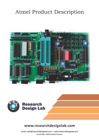
  • 2. RESEARCH DESIGN LABS | VOLUME 1, ISSUE 1 WWW.RESEARCHDESIGNLAB.COM All digital circuits require regulated power supply. Here is a simple power supply circuit diagram used on this board. You can use AC or DC source (12V) which converts into regulated 5V which is required for driving the developmentboard circuit. Select the IC's from the given list and mount on the ZIF socket. ZIF socket pin maps out PORT1 PORT2 PORT3 PORT4 for easy making connections for the restof the circuit. Port 1 is enabled with pull up circuit and also connected ISP for easy on board Programming. 1. Power supply, 5V-12V 1. 40 pin ZIF socket for IC mount & ISP connector* NOTE: if you are following to on board program, the capacitor c1 should be desoldered and removed from the port. You also need to know, if you remove the capacitor the board has to reset manually by pressing the reset button s1 each time you burn a code.
  • 3. Resets your microcontroller by pressing s1 NOTE: if you are following to on board program, the capacitor c1 should be desoldered and removed from the port. You also need to know, if you remove the capacitor the board has to reset manually by pressing the reset button s1 each time you burn a code. 2. Reset Node connector is an additional on board connection extender or 1 connection IN and 1 connection out 3. Node connector One seven segment digit consist of 7+1 LEDs which are arranged in a specific formation which can be used to represent digits from 0 to 9 and even some letters. One additional LED is used for marking the decimal dot, in case you want to write a decimal point in the desired segment. 4. 4 digit 7 segment display
  • 4. 26 Pin raspberry connector is an easy way for making connections with raspberry pi with this development board. 5. 26 pin raspberry connector 6. Arduino Shield footprint Arduino Shield footprint is provided in the board to mount different types of Arduino compatible shields on this development board. IC ULN2803 consists of octal high voltage, high current darlington transistor arrays. The eight NPN Darlington connected transistors in this family of arrays are ideally suited for interfacing between low logic level digital circuitry (such as TTL, CMOS or PMOS/NMOS) and the higher current/voltage requirements of lamps, relays, printer hammers or other similar loads for a broad range of computer, industrial, and consumer applications. 7. ULN 2803 driver · Eight Darlingtons with Common Emitter. · Open–collector outputs. · Free wheeling clamp diodes for transient suppression. Features · Output Current to 500 mA. · Output Voltage to 50 V. · Inputs pinned opposite outputs to simplify board layout.
  • 5. The ULN 2803 IC consists of eight NPN Darlington connected transistors (often called a Darlington pair). Darlington pair consists of two bipolar transistors such that the current amplified by the first is amplified further by the second to get a high current gain β or hFE. The figure shown below is one of the eight Darlington pairs of ULN 2803 IC. Now 2 cases arise:- Case 1: When IN is 0 volts. Q1 and Q2 both will not conduct as there is no base current provided to them. Thus, nothing will appear at the output (OUT). Case 2: When IN is 5 volts. Input current will increase and both transistors Q1 and Q2 will begin to conduct. Now, input current of Q2 is combination of input current and emitter current of Q1, so Q2 will conduct more than Q1 resulting in higher current gain which is very much required to meet the higher current requirements of devices like motors, relays etc. Output current flows through Q2 providing a path (sink) to ground for the external circuit that the output is applied to. Thus, when a 5V input is applied to any of the input pins (1 to 8), output voltage at corresponding output pin (11 to 18) drops down to zero providing GND for the external circuit. Thus, the external circuit gets grounded at one end while it is provided +Vcc at its other end. So, the circuit gets completed and starts operating. Working
  • 6. One IC that wants to talk to another must: (Protocol) 1) Wait until it sees no activity on the I2C bus. SDAand SCLare both high. The bus is 'free'. 2) Put a message on the bus that says 'its mine' - I have STARTED to use the bus. All other ICs then LISTEN to the bus data to see whether they might be the one who will be called up (addressed). 3) Provide on the CLOCK (SCL) wire a clock signal. It will be used by all the ICs as the reference time at which each bit of DATA on the data (SDA) wire will be correct (valid) and can be used. The data on the data wire (SDA) must be valid at the time the clock wire (SCL) switches from 'low' to 'high' voltage. 4) Put out in serial form the unique binary 'address'(name) of the IC that it wants to communicate with. 5) Put a message (one bit) on the bus telling whether it wants to SEND or RECEIVE data from the other chip. (The read/write wire is gone!) 6) Ask the other IC to ACKNOWLEDGE (using one bit) that it recognized its address and is ready to communicate. 7)After the other IC acknowledges all is OK, data can be transferred. 8) The first IC sends or receives as many 8-bit words of data as it wants. After every 8-bit data word the sending IC expects the receiving IC to acknowledge the transfer is going OK. 9) When all the data is finished the first chip must free up the bus and it does that by a special message called 'STOP'. It is just one bit of information transferred by a special 'wiggling' of the SDA/SCLwires of the bus. 1.I2C bus
  • 7. Serial to Peripheral Interface (SPI) is a hardware/firmware communications protocol developed by Motorola and later adopted by others in the industry. Microwire of National Semiconductor is same as SPI. Sometimes SPI is also called a "four wire" serial bus. The Serial Peripheral Interface or SPI-bus is a simple 4-wire serial communications interface used by many microprocessor/microcontroller peripheral chips that enables the controllers and peripheral devices to communicate each other. Even though it is developed primarily for the communication between host processor and peripherals, a connection of two processors via SPI is just as well possible. The SPI bus, which operates at full duplex (means, signals carrying data can go in both directions simultaneously), is a synchronous type data link setup with a Master / Slave interface and can support up to 1 megabaud or 10Mbps of speed. Both single-master and multi-master protocols are possible in SPI. But the multi-master bus is rarely used and look awkward, and are usually limited to a single slave. The SPI Bus is usually used only on the PCB. There are many facts, which prevent us from using it outside the PCB area. The SPI Bus was designed to transfer data between various IC chips, at very high speeds. Due to this high-speed aspect, the bus lines cannot be too long, because their reactance increases too much, and the Bus becomes unusable. However, its possible to use the SPI Bus outside the PCB at low speeds, but this is not quite practical. The peripherals can be a Real Time Clocks, converters like ADC and DAC, memory modules like EEPROM and FLASH, sensors like temperature sensors and pressure sensors, or some other devices like signal-mixer, potentiometer, LCD controller, UART, CAN controller, USB controller and amplifier. 1.SPI bus
  • 8. All XBeeZNet 2.5 modules can be identified by their unique 64-bit addresses or a user- configurableASCII string identifier The 64-bit address of a module can be read using the SH and SL commands. TheASCII string identifier is configured using the NI command. To transmit using device addressing, only the destination address must be configured. The destination address can be specified using either the destination device's 64-bit address or its NI- string. The XBee modules also support coordinator and broadcast addressing modes. Device addressing in the AT firmware is configured using the DL, DH, or DN commands. In the API firmware, the ZigBee Transmit Request API frame (0x10) can be used to specify destination addresses. To address a node by its 64-bit address, the destination address must be set to match the 64-bit address of the remote. In the AT firmware, the DH and DL commands set the destination 64-bit address. In the API firmware, the destination 64-bit address is set in the ZigBee Transmit Request frame. ZigBee end devices rely on a parent (router or coordinator) to remain awake and receive any data packets destined for the end device. When the end device wakes from sleep, it sends a transmission (poll request) to its parent asking if the parent has received any RF data destined for the end device. The parent, upon receipt of the poll request, will send an RF response and the buffered data (if present). If the parent has no data for the end device, the end device may return to sleep, depending on its sleep mode configuration settings. The following figure demonstrates how the end device uses polling to receive RF data through its parent. 1.XBEE footprint/ XBEE Adaptor module
  • 9. These connectors provide on board 3.3V DC connections. A s t a n d a r d F T 2 3 2 breakout board from researchdesignlab.com could be used to interface on these connectors, whose other end is connected to a USB. RS-232 is a standard communication protocol for linking computer and its peripheral devices to allow serial data exchange. In simple terms RS232 defines the voltage for the path used for data exchange between the devices. It specifies common voltage and signal level, common pin wire configuration and minimum, amount of control signals. 1.DB-9 female connector 11. FT232 breakout board connector 12. DC 3.3V connectors
  • 10. 1. 8x1 LED's LED's are used to indicate something, whether any pin is high or indicating the output for many purposes like indicating I/O status or program debugging running state. We have four led outputs on board which can be used by the programmer as per the requirement for testing and development. 1. 8 way DIP switch DIP switches are an alternative to jumper blocks. Their main advantages are that they are quicker to change and there are no parts to lose.
  • 11. 1. RTC Module The DS1307 Serial Real Time Clock is a low power, full BCD clock/calendar plus 56 bytes of nonvolatile SRAM. Address and data are transferred serially via a 2-wire bi- directional bus. The clock/calendar provides seconds, minutes, hours, day, date, month, and year information. The end of the month date is automatically adjusted for months with less than 31 days, including corrections for leap year. The clock operates in either the 24-hour or 12-hour format with AM/PM indicator. The DS1307 has a built- in power sense circuit which detects power failures and automatically switches to the battery supply. OPERATION The DS1307 operates as a slave device on the serial bus. Access is obtained by implementing a START condition and providing a device identification code followed by a register address. Subsequent registers can be accessed sequentially until a STOP condition is executed. When VCC falls below 1.25 x VBAT the device terminates an access in progress and resets the device address counter. Inputs to the device will not be recognized at this time to prevent erroneous data from being written to the device from an out of tolerance system. When VCC falls below VBAT the device switches into a low current battery backup mode. Upon power up, the device switches from battery to VCC when VCC is greater than VBAT +0.2V and recognizes inputs. Features: 1. 56 byte nonvolatile RAM for data storage 2. 2-wire serial interface 3. Programmable square wave output signal 4. Automatic power-fail detect and switch circuitry 5. Consumes less than 500 nA in battery backup mode with oscillator running 6. Optional industrial temperature range -40°C to +85°C 7. Available in 8-pin DIP or SOIC 8. Recognized by Underwriters Laboratory
  • 12. PIN DESCRIPTION 1. VCC - Primary Power Supply 2. X1, X2 - 32.768 kHz Crystal Connection 3. VBAT - +3V Battery Input 4. GND - Ground 1.EEPROM IC, EEPROM I2C 4K, 24C04, DIP8 Memory Size: 4Kbit Memory Configuration: 512 x 8 Interface Type: I2C, Serial Clock Frequency: 400kHz Supply Voltage Range: 2.5V to 5.5V Memory Case Style: DIP No. of Pins: 8 Operating Temperature Range: -40°C to +85°C SVHC: No SVHC (19-Dec-2011) Base Number: 24 Device Marking: M24C04 IC Generic Number: 24C04 Interface: I2C Interface Type: Serial, I2C Logic Function Number: 24C04 Memory Configuration: 512 x 8 Memory Size: 4Kbit Memory Type: EEPROM Memory Voltage Vcc: 2.5V Operating Temperature Max: +85°C Operating Temperature Min: -40°C Package / Case: DIP Supply Voltage Max: 5.5V Supply Voltage Min: 2.5V Termination Type: Through Hole Voltage Vcc: 2.5V 5. SDA - Serial Data 6. SCL - Serial Clock 7. SQW/OUT - Square wave/Output Driver
  • 13. 1. 2x5x2 jumper node Node connector is an additional on board connection extender or 1 connection IN and 1 connection out 1. DC 5V connectors These connectors provide on board 5V DC connections. 1. Analog to Digital output Most of the signals directly encountered in science and engineering are continuous: light intensity that changes with distance; voltage that varies over time; a chemical reaction rate that depends on temperature, etc. Analog-to-Digital Conversion (ADC) and Digital-to-Analog Conversion (DAC) are the processes that allow digital computers to interact with these everyday signals. Digital information is different from its continuous counterpart in two important respects: it is sampled, and it is quantized. Both of these restrict how much information a digital signal can contain.
  • 14. FUNCTIONAL DESCRIPTION Addressing Each PCF8591 device in an I2C-bus system is activated by sending a valid address to the device. The address consists of a fixed part and a programmable part. The programmable part must be set according to the address pins A0, A1 and A2. The address is always sent as the first byte after the start condition in the I2C-bus protocol. The last bit of the address byte is the read/write-bit which sets the direction of the following data transfer. D/A CONVERSION The third byte sent to a PCF8591 device is stored in the DAC data register and is converted to the corresponding analog voltage using the on-chip D/A converter. This D/A converter consist of a resistor divider chain connected to the external reference voltage with 256 taps and selection switches. The tap decoder switches one of these taps to the DAC output line. The analog output voltage is buffered by an auto-zeroed unity gain amplifier. Setting the analog output enable flag of the control register switches this buffer amp on or off. In the active state, the output voltage is held until a further data byte is sent. The on-chip D/A converter is also used for successive approximation A/D conversion. In order to release the DAC for an A/D conversion cycle the unity gain amplifier is equipped with a track and hold circuit. This circuit holds the output voltage while executing the A/D conversion. A/D CONVERSION The A/D converter uses the successive approximation conversion technique. The on-chip D/A converter and a high-gain comparator are used temporarily during an A/D conversion cycle. An A/D conversion cycle is always started after sending a valid read mode address to a PCF8591 device. The A/D conversion cycle is triggered at the trailing edge of the acknowledge clock pulse and is executed while transmitting the result of the previous conversion Once a conversion cycle is triggered, an input voltage sample of the selected channel is stored on the chip and is converted to the corresponding 8-bit binary code. Samples picked up from differential inputs are converted to an 8-bit two's complement code. The conversion result is stored in the ADC data register and awaits transmission. If the auto-increment flag is set, the next channel is selected. The first byte transmitted in a read cycle contains the conversion result code of the previous read cycle. After a POR condition, the first byte read is 80h.The maximum A/D conversion rate is given by the actual speed of the I2C-bus
  • 15. PCF8951T The PCF8591 is a single-chip, single-supply low-power 8-bit CMOS data acquisition device with four analog inputs, one analog output and a serial I2C-bus interface. Three address pins A0, A1 and A2 are used for programming the hardware address, allowing the use of up to eight devices connected to the I2C-bus without additional hardware. Address, control and data to and from the device are transferred serially via the two-line bidirectional I2C- bus.The functions of the device include analog input multiplexing, on-chip track and hold function, 8-bit analog-to-digital conversion and an 8-bit digital-to-analog conversion. The maximum conversion rate is given by the maximum speed of the I2C-bus. FEATURES 1. Single power supply 2. Operating supply voltage 2.5 V to 6.0 V 3. Low standby current 4. Serial input and output via I2C-bus 5. I2C address selection by 3 hardware address pins 6. Max sampling rate given by I2C-bus speed 7. 4 analog inputs configurable as single ended or differential inputs 8. Auto-incremented channel selection 9. Analog voltage range from VSS to VDD 10. On-chip track and hold circuit 11. 8-bit successive approximation A/D conversion 12. Multiplying DAC with one analog output Fig: PCF8951T IC PIN DESCRIPSION 1-4. AIN0- AIN3:-analog inputs (A/D converter) 5-7. A0- A2:- hardware slave address 8. VSS: - ground supply voltage 9. SDA: - I2C-bus serial data input and output 10. SCL: - I2C-bus serial clock input 11. OSC: - oscillator input/output 12. EXT: - external/internal switch for oscillator input 13. AGND: - analog ground supply 14. VREF: - voltage reference input 15. AOUT: - analog output (D/A converter) 16. VDD: - supply voltage
  • 16. 1. 4x1 keypad Switches are mainly used to switch the controls of a module. We have four switches on board which can be used by the programmer as per the requirement for testing and development. 1. 16x2 LCD connectors LCD screen consists of two lines with 16 characters each. Each character consists of 5x7 dot matrix. Contrast on display depends on the power supply voltage and whether messages are displayed in one or two lines. For that reason, variable voltage 0-Vdd is applied on pin marked as Vee. Trimmer potentiometer is usually used for that purpose. Some versions of displays have built in backlight (blue or green diodes). When used during operating, a resistor for current limitation should be used (like with any LE diode). LCD Connection Depending on how many lines are used for connection to the microcontroller, there are 8-bit and 4-bit LCD modes. The appropriate mode is determined at the beginning of the process in a phase called “initialization”. In the first case, the data are transferred through outputs D0-D7 as it has been already explained. In case of 4-bit LED mode, for the sake of saving valuable I/O pins of the microcontroller, there are only 4 higher bits (D4-D7) used for communication, while other may be left unconnected. Consequently, each data is sent to LCD in two steps: four higher bits are sent first (that normally would be sent through lines D4-D7), four lower bits are sent afterwards. With the help of initialization, LCD will correctly connect and interpret each data received. Besides, with regards to the fact that data are rarely read from LCD (data mainly are transferred from microcontroller to LCD) one more I/O pin may be saved by simple connecting R/W pin to the Ground. Such saving has its price. Even though message displaying will be normally performed, it will not be possible to read from busy flag since it is not possible to read from display.
  • 17. Features: 1. Can display 224 different symbols. 2. Low power consumption. 3. 5x7 dot matrix format. 4. Powerful command set and user produced characters. Fig: Circuit connections of LCD PIN DESCRIPTION 1. Gnd:- Power supply ground 2. VCC:-+5v Power supply input 3. RS:- Reset pin 4. R/W:- Read/Write pin 5. En:-Enable pin 6. D0-D7:- Data lines
  • 18. 1. Node connector Node connector is an additional on board connection extender or 1 connection IN and 1 connection out 1. 4x4 Matrix Keypad In a 4x4 matrix keypad eight Input/Output ports are used for interfacing with any microcontrollers. Rows are connected to Peripheral Input/Output (PIO) pins configured as output. Columns are connected to PIO pins configured as input with interrupts. In thisconfiguration, four pull-up resistors must be added in order to apply a high level on the corresponding input pins as shown in below Figure. The corresponding hexadecimal value of the pressed key is sent on four LEDs. WORKING This Application Note describes programming techniques implemented on the AT91 ARM- based microcontroller for scanning a 4x4 Keyboard matrix usually found in both consumer and industrial applications for numeric data entry.AT91 Keyboard interface In this application, a 4x4 matrix keypad requiring eight Input/Output ports for interfacing is used as an example. Rows are connected to Peripheral Input/Output (PIO) pins configured as output. Columns are connected to PIO pins configured as input with interrupts. In this configuration, four pull-up resistors must be added in order to apply a high level on the corresponding input pins as shown in Figure 1. The corresponding hexadecimal value of the pressed key is sent on four LEDs.
  • 19. FEATURES 1. Contact debouncing. 2. Easy to interface. 3. Interfaces to any microcontroller or microprocessor. 4. Data valid output signal for interrupt activation. 1.DC 12V connectors These connectors provide on board 12V DC connections. PIN DETAILS pin 1-4: R0-R3:- Rows pin 5-8: C0-C3:- Columns